Thursday, August 6, 2015

the physicists' war

Nature Magazine just dropped a great historical commentary (open access!) on the "Physicists' War," that would be World War II, and which today is the 70th anniversary of the atomic destruction of Hiroshima. World War I is known the "Chemists' War" due to the prevalence of chemical weapons such as phosgene, chlorine, and mustard gas. So clearly, WWII was the "Physicists' War" because of the development of radar and the atom bomb right? You and me both were wrong, and this article details the (reverse?) misnomer.

The misnomer began shortly after WWII. Because the deployment of the atomic bomb needed to be explained to the American public, while protecting the top secret information used to make it, the declassified "Smyth Report" detailed not the nuts and bolts of engineering and manufacturing an atomic bomb, but rather the theoretical physics behind its operation, which was unclassified and widely known by the physics community at the time. A 1949 Life magazine profile of J. Robert Oppenheimer, the "Father of the Atomic Bomb," highlighted the importance of physics in winning this effort. That and the development of radar at MIT's Radiation Laboratory cemented the notion of WWII as the Physicists' War. 

But the term was actually coined four years earlier by James Conant, Harvard President and chair of the US National Defense Research Committee. And far be it for a highly ranked official to give the game away about the Allies plans regarding wartime physics, especially given that MIT's 'Rad Lab' was a year old and the Manhattan Project wasn't a project yet, he actually meant something quite different. He meant education


Knowledge not nukes [Technique/MIT Museum]
Specifically, the education of servicemen in the basics of electricity, circuits, optics, and radio was imperative for the US to compete in modern warfare. For a taste of the other skills in demand, "[the] army, for example, wanted the new courses to emphasize how to measure lengths, angles, air temperature, barometric pressure, relative humidity, electric current and voltage. Lessons in geometrical optics would emphasize applications to battlefield scopes; lessons in acoustics would drop examples from music in [favor] of depth sounding and sound ranging." So much so that courses in atomic and nuclear physics were suspended for the remainder of the war, for not being "essential." Oh that and physics instructors, like many other natural resources, found themselves subject to rationing. Poaching and hoarding of physics teachers was discouraged to the point of criminality, and quality control was mandated by ratios of proper to converted instructors. And there were even teaching-related deferments for said instructors.

Well that's a nice historical curiosity and all, but I'm sure the lasting effects were short-lived and inconsequential. And that would also happen to be wrong! After the war, physicists both benefited from increased government funding of laboratories and training, and suffered at the hands of anti-Communists during the Red Scare. Many decades following (and I've heard this from more senior coworkers), the practice of physics was associated with war. The increased government funding also altered the relationship between national defense and academia, and the way scientific research is organized and funded to this day. And historical decisions continue to be fascinating.
Sunday, August 2, 2015

7nm node

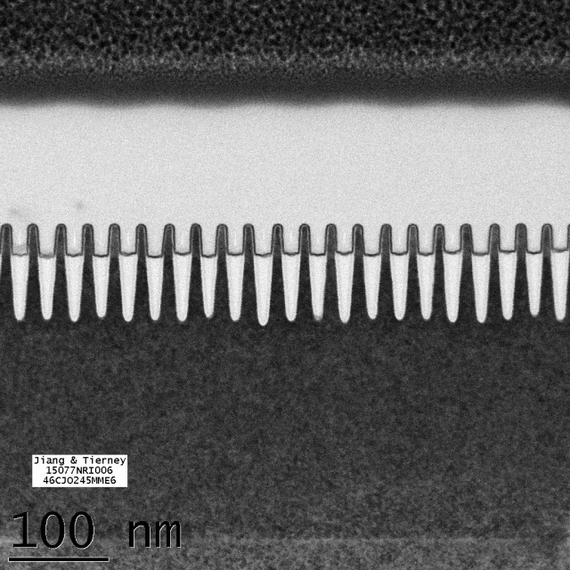
Recently, IBM announced the fabrication of the 7nm node, packing transistors about four times as dense as current technology, surprising you and me both who thought that IBM didn't make things anymore. IBM had just paid semiconductor behemoth GlobalFoundries 1.5 billion dollars to take its (IBM's!!!) fabrication plants (Fabs) off their hands.

While ambiguous in terms of the actual dimension being measured here, the 7nm node roughly corresponds to the smallest feature measuring 7nm, with one nanometer (=nm) roughly one hundred thousandth the width of a human hair, which sounds cool cause it's really small. Transistors have routinely been made with smaller dimensions, as I routinely made transistors out of carbon nanotubes in grad school (the 1nm node, I suppose), however IBM's got a wafer-full of them here that actually work, not an easy feat, and certainly not something I came anywhere near achieving (nor was trying to).


Even-spaced 7nm node transistors, where 7nm corresponds to the tiny spacing between them [IBM Research]
Moore's Law was christened by Gordon Moore, the original CEO of Intel, who predicted that the number of transistors on a chip would double roughly every 18 months, and has surprisingly proven true over the past 50 years. Very surprising given the amount of technological advancement that had to happen. The flip-side of that prediction is that a Fab would double in price at the same rate, and hence the recent consolidation and divestiture of chip-making plants. Now couple that with Moore's Law running head-first into limits set by physics, and it becomes a big deal.

The delightfully eponymous Patrick Moorhead, a chip technology analyst, said "I believe Intel has done the same thing already [... they're] just not telling people." I'm sure many of my fellow Illinois physics graduates currently employed at Intel's research Fab outside Portlandia are working on said venture, but they won't tell me either. Intel believes the 7nm node will be the last one scalable to wafer-level production with silicon (and to be fair, IBM used an alloy of silicon and germanium).

And it took leaps and bounds just to where we are. Chips are made using optical lithography, akin to old school photography, whereby light-sensitive resists are exposed through a mask, breaking down the resist that's projected through and leaving intact that in the shadows. This gives you feature sizes on the order of the wavelength of light being used, the current industry standard being down in the ultraviolet at 193nm. However, that computer you just bought has chips at the 14nm node, so engineers have done a helluva job squeezing every last bit of resolution out of those photons. As Doug Natelson of Nanoscale Views notes, "[manufacturers] have relied on several bits of extreme cleverness to pattern features down to 1/20 of the free-space wavelength of the light, including immersion lithography, optical phase control, exotic photochemistry, and multiple patterning." IBM made the switch to extreme UV technology (with a wavelength of 13.5nm) to achieve the 7nm node, but of course that came with its own batch of headaches. Those that are particularly painful include powering the laser source and the fact that it's really hard to do optics at that small of wavelength. Which is also why it'll be a few years before the actual manufacturing of these 7nm chips will begin.

It's difficult to predict what happens past the 7nm node, should silicon no longer prove viable. Carbon-based electronics, in the form of nanotubes and graphene, have been much touted for the past decade, but that seems to have fizzled out. Graphene's siblings, silicene, germanene, and black phosphorous, are currently the subjects of ongoing research, as are its wonderful cousins, the similarly thin transition metal dichalcogenides. Different architectures for computing are also in the works as the field of spintronics and magnonics seek to use the spin of the electron to carry information, as opposed to the charge as is done now. And then there's quantum computing, which promises to efficiently solve certain classes of problems, so that's just like different, man.

IBM stock price has dipped $1.84 to $162.01 a share since the announcement.